Combinational and Sequential Circuits
Digital systems are built from two ideas: logic that computes from the inputs right now, and storage that remembers a state until the next clock event. The boundary between these two ideas explains adders, multiplexers, registers, counters, CPUs, and FPGA designs.
Learning Objectives
By the end of this lesson, you should be able to distinguish combinational and sequential circuits, identify where memory exists in a digital block, explain propagation delay and clocked updates, and sketch a simple state-machine style system.
Combinational Circuits
A combinational circuit has no memory. Its output is a Boolean function of the present inputs only.
$$
Y = f(A, B, C, ...)
$$
Examples include adders, decoders, encoders, multiplexers, comparators, parity generators, and simple arithmetic logic. If the inputs return to the same values, the outputs return to the same values after propagation delay.
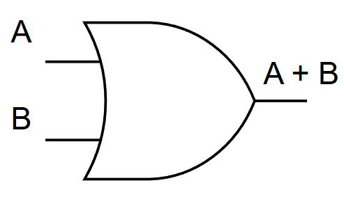
For a half adder:
$$
S = A \oplus B
$$
$$
C_{out} = A \cdot B
$$
The equations do not include time, previous state, or a clock. That is the defining property.
Sequential Circuits
A sequential circuit has memory. Its next output or next state depends on the current inputs and the stored state.
$$
Q_{next} = f(Q_{present}, Inputs)
$$
Registers, counters, shift registers, memory arrays, and finite state machines are sequential circuits. A clocked flip-flop samples its input at a clock edge and holds the value between edges.
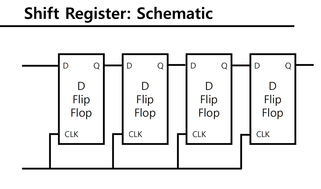
For a D flip-flop:
$$
Q_{next} = D \quad \text{at the active clock edge}
$$
Timing Matters
Combinational logic is not instantaneous. It has propagation delay, usually written as t_pd. Sequential logic also needs setup and hold time around the clock edge.
t_pd: input change to output change.t_setup: data must be stable before the clock edge.t_hold: data must remain stable after the clock edge.T_clk: clock period.
A simplified single-clock timing rule is:
$$
T_{clk} \ge t_{CQ} + t_{logic} + t_{setup} + margin
$$
where t_CQ is clock-to-Q delay and t_logic is the delay through combinational logic between registers.
Building Real Systems
A counter uses registers to store the present count and combinational logic to calculate the next count. A CPU datapath uses registers for values and combinational logic for ALU operations. An FPGA design uses LUTs for combinational logic and flip-flops for state.
Worked Example: 2-Bit Counter
A synchronous 2-bit up counter stores Q1 Q0. The next-state logic is:
$$
D_0 = \overline{Q_0}
$$
$$
D_1 = Q_1 \oplus Q_0
$$
At each clock edge, the flip-flops load D1 D0, producing 00 -> 01 -> 10 -> 11 -> 00. The XOR and inverter are combinational; the flip-flops are sequential.
Common Mistakes
- Expecting gates alone to remember a value.
- Forgetting that combinational outputs still have propagation delay.
- Building feedback loops without intentional storage.
- Mixing clock domains without synchronizers.
- Ignoring reset behavior in counters and FSMs.
Practical Checks
When reviewing a digital circuit, ask where the state is stored, which clock updates it, whether all paths meet setup and hold timing, whether reset puts the circuit into a known state, and whether combinational outputs are allowed to glitch.
Summary
Combinational circuits compute; sequential circuits remember. Real digital systems combine both: registers hold state, combinational logic calculates next values, and clocks make updates predictable.
Further Reading
- Harris and Harris, Digital Design and Computer Architecture.
- Texas Instruments logic application notes on flip-flops, counters, and timing.
- FPGA vendor timing-closure guides for setup, hold, and clock-to-Q terminology.